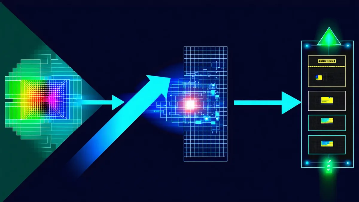
This walkthrough covers the Photoniq verification workflow from first layout import to reading the structured output report. It's intended for PIC design engineers who are evaluating the tool for the first time, or for tape-out engineers setting up the verification step in a new design flow. The steps here reflect the current Photoniq CLI and API behavior as of early 2026.
What You Need Before Starting
Photoniq verification requires three inputs:
- GDS-II layout file — the tape-out-candidate layout in GDS-II (or OASIS) format. This is typically exported from KLayout, Cadence Virtuoso, or a Python-based PIC design environment like gdsfactory or Luceda IPKISS.
- Reference netlist — the schematic-level optical connectivity, in SPICE netlist format or Photoniq's native
.pnq_netJSON format. For designs built in Virtuoso, this is the exported netlist from the schematic editor. For gdsfactory designs, the connectivity netlist can be exported from the Python design representation. - PDK specification — a
pdk_config.jsonfile that maps GDS layer numbers to physical layer names, specifies component port metadata, and encodes photonic rule deck thresholds. Photoniq ships pre-built PDK configs for supported foundry PDKs; for custom PDKs, the config format is documented in the PDK support guide.
If you're evaluating with an existing design but don't have a formal reference netlist, Photoniq can run in "layout-only" mode, which performs DRC-class checks and optical rule checks without the LVS connectivity comparison. This is useful for catching the most common violation types even without a schematic reference.
Step 1: Install and Authenticate
The Photoniq CLI is distributed as a Python package. Install it with:
pip install photoniq-sdkAfter installation, authenticate with your Photoniq account (required for verification runs beyond the Starter tier limit):
photoniq auth login
# Opens browser or prompts for API key
# API key available from your Photoniq account dashboard

photoniq auth status
# Output: Authenticated as [email protected] (Professional plan)
The authentication stores a local credential file at ~/.photoniq/credentials. For CI/CD environments, set the environment variable PHOTONIQ_API_KEY instead of using interactive login.
Step 2: Validate Your Inputs
Before submitting a verification job, run the input validation command. This checks that the GDS file is readable, the PDK config is syntactically correct, and the netlist format is supported. It does not run any verification checks — it just confirms the inputs are structurally valid:
photoniq validate \
  --gds design/mzm_chip_rev5.gds \
  --netlist schematic/mzm_chip.spi \
  --pdk pdk/imec_isipp50g_v2.3.json

# Output:
# [OK]  GDS file: 1 top cell (MZM_CHIP_TOP), 142 cells, 3 layers
# [OK]  PDK config: 28 components, 6 rule checks
# [OK]  Netlist: 18 component instances, 24 nets
# [WARN] PDK version 2.3 → latest available is 2.4 (run with --pdk-update to fetch)
# Validation passed. Ready to submit.
The PDK version warning is important: if the foundry has released a PDK update with revised rule thresholds, running against the old version may produce results that don't reflect the current tape-out requirements. Use --pdk-update to pull the latest version, then re-validate to confirm inputs are still compatible.
Step 3: Submit the Verification Job
photoniq verify \
  --gds design/mzm_chip_rev5.gds \
  --netlist schematic/mzm_chip.spi \
  --pdk pdk/imec_isipp50g_v2.4.json \
  --output reports/ \
  --format json,html

# Output:
# Submitting verification job...
# Job ID: job_8f3a2c19
# Queued. Estimated runtime: 4-8 minutes for this design complexity.
# Polling for completion... (Ctrl+C to detach, results will be available at job ID)
#
# [1 min] Running GDS extraction...
# [2 min] Running photonic LVS...
# [4 min] Running optical rule checks...
# [5 min] Generating report...
# Verification complete. 2 HIGH violations, 4 MEDIUM violations, 7 INFO items.
# Reports saved to reports/job_8f3a2c19_report.json and reports/job_8f3a2c19_report.html
For large designs (complex chips with hundreds of components), the job may take 15–30 minutes. The --detach flag submits the job and exits immediately, allowing you to retrieve results later with photoniq jobs get job_8f3a2c19. For CI pipelines, --fail-on HIGH causes the CLI to exit with code 1 if any HIGH-severity violations are found, which automatically fails the CI job.
Step 4: Reading the Verification Report
The structured JSON report contains one record per violation. A representative HIGH-severity violation record looks like this:
{
  "job_id": "job_8f3a2c19",
  "pdk": "imec_isipp50g_v2.4",
  "violations": [
    {
      "violation_id": "V_0012",
      "check_type": "MODE_MISMATCH",
      "severity": "HIGH",
      "cell": "MZM_CHIP_TOP/MZM_ARM_A/WG_CONNECT_003",
      "layer": "WG_CORE (1/0)",
      "coordinate": { "x": 42350, "y": 18820 },
      "description": "Width discontinuity at port junction. Port WG_CONNECT_003:output (500 nm) connects to MODULATOR_ACCESS_01:input (600 nm). No taper cell present at this junction. Expected: taper_linear_500_600_v1 or equivalent.",
      "suggested_fix": "Insert PDK taper cell taper_linear_500_600_v1 between WG_CONNECT_003 and MODULATOR_ACCESS_01.",
      "optical_impact_estimate": "Junction loss in range 0.1–0.4 dB (width delta 100 nm, abrupt transition)"
    }
  ]
}
Each HIGH violation has: the cell hierarchy path where it occurs, the GDS layer and coordinate for navigation in KLayout, a description explaining exactly what was found, a suggested fix (usually a specific PDK cell insertion or parameter correction), and an optical impact estimate based on the PDK model for this violation type.
The HTML report presents the same data in a layout-viewer-friendly format. Clicking a violation entry copies the GDS coordinate to the clipboard in a format that KLayout accepts directly in the coordinate jump field — a small UX detail that saves time during triage.
Step 5: Fixing Violations and Re-Running
The typical fix cycle for HIGH violations is:
- Open the report HTML in a browser. Review the violation list by severity.
- For each HIGH violation, use the GDS coordinate to navigate to the location in KLayout.
- Implement the suggested fix — usually a cell insertion, cell substitution, or parameter correction.
- Export the updated GDS-II from the layout tool.
- Re-run
photoniq verifywith the updated GDS.
In practice, most designs surface 2–5 HIGH violations on the first verification run of a mature layout revision — not because the design is poorly executed, but because some categories of photonic violations are invisible to conventional checking tools and accumulate silently during layout assembly. The first verification run establishes the baseline; subsequent runs on the same design converge rapidly as the systematic issues are resolved.
What the Report Does Not Tell You
We're not saying a clean Photoniq verification report means your chip will work. Verification confirms geometric compliance with PDK optical rules — it does not simulate optical performance. A report with zero violations means:
- All waveguide junctions have compliant width matching.
- All coupling gaps are within PDK specification.
- All taper structures meet adiabatic length and angle requirements.
- Layout connectivity matches schematic connectivity (LVS clean).
- No proximity cross-talk risks above PDK threshold.
It does not mean the optical transfer function matches your simulation, that resonance wavelengths are aligned to a WDM grid, or that the chip meets the optical link budget for the intended system application. Those require simulation (Lumerical INTERCONNECT, a circuit-level Python model) and an optical loss budget analysis against the system specification. Verification is one layer of the pre-tape-out stack; simulation and loss budget analysis are the other layers.
Integrating into Your Tape-Out Checklist
For teams with an established tape-out checklist, Photoniq fits as a specific line item after DRC and before the final foundry submission package preparation:
Tape-out checklist:
[x] Geometric DRC: PASS (0 violations, 2 waived with sign-off)
[x] SPICE LVS: PASS
[ ] Photoniq photonic verification: target PASS or 0 HIGH violations
[ ] Optical loss budget: all critical paths within budget
[ ] Final GDS export and submission package assembly
Setting up the PDK config file for a specific foundry PDK is a one-time effort per PDK version. Once the config is established and validated, running Photoniq verification on successive design revisions takes the same three commands — validate, verify, review report — and scales to the full design complexity without additional setup. The value per run compounds: teams that run verification on every revision of a design in the months before tape-out accumulate a documented verification history that demonstrates engineering discipline at every step of the tape-out preparation process.