The process design kit is the contract between the designer and the foundry. When you design a PIC using a foundry's PDK, you're working within a defined set of guarantees: that the process layers will be fabricated to the specified tolerances, that the component models accurately describe fabricated device behavior within the process window, and that a layout which passes the PDK rule deck will be manufacturable without modification.
Understanding what's actually inside that rule deck — its structure, its coverage, and its limitations — is essential for anyone building a verification flow on top of it. The PDK rule deck is not just a DRC file. For photonic verification, it's the ground truth that defines what constitutes a correct layout.
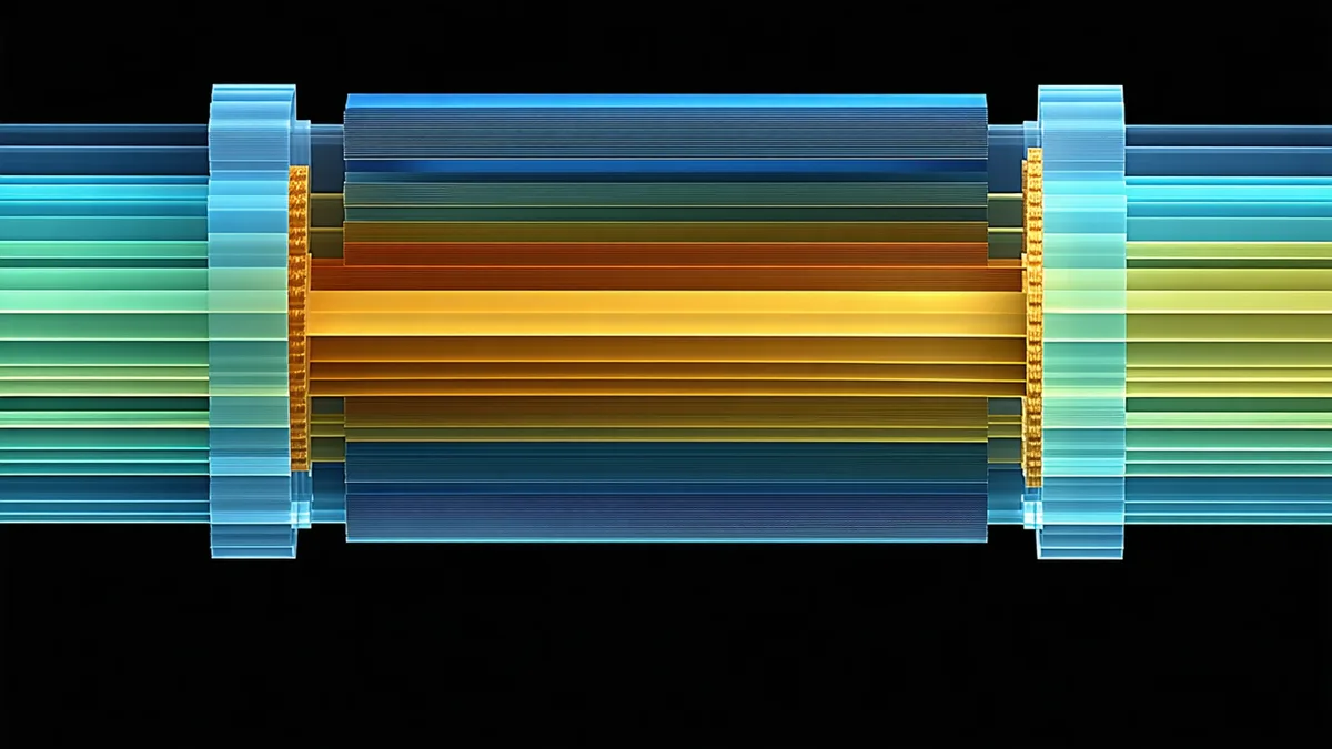
Anatomy of a PIC PDK
A complete silicon photonics PDK typically consists of several distinct components, each serving a different verification purpose:
Layer stack definition
The layer stack specifies which physical layers exist in the process — silicon waveguide layer, partial etch (rib) layer, silica cladding, metal layers, doped regions for p-n junction modulators, germanium for photodetectors — and maps each to GDS-II layer/datatype numbers. This mapping is foundational: a waveguide drawn on layer 1/0 in one PDK may be on layer 3/0 in another. Verification tools must read the layer stack to interpret what each polygon in the GDS-II file physically represents.
Geometric design rules
Geometric DRC rules specify the minimum feature sizes, spacing requirements, and enclosure rules that the fabrication process can reliably achieve. For a silicon photonics process, these include: minimum waveguide width, minimum gap between adjacent waveguides, minimum etch depth for partial-etch regions, minimum metal line width and spacing, and minimum overlap between layers (e.g., silicide blocking over n-implant). These are the rules that conventional DRC tools check — polygon geometry against numerical thresholds — and they apply to PICs in the same way as to CMOS.
Component library with PDK port metadata
A photonics PDK component library extends beyond the CMOS standard cell concept in an important way: each component declares optical ports with physical attributes. A PDK waveguide bend cell declares its access ports with width, layer, and polarization type. A PDK grating coupler cell declares its fiber-side port with the expected fiber mode field diameter and coupling angle, and its on-chip port with its waveguide width and layer. This metadata is what enables optical verification: it provides the ground truth for what each port expects from what it connects to.
The photonic rule deck
Beyond geometric DRC, a photonic PDK may include a photonic rule deck that specifies optical-specific rules. These are the rules that make photonic verification distinct from conventional CMOS verification. They include: minimum coupling gap for each coupler structure (defined per coupling ratio target), allowed waveguide width ranges for single-mode operation at the target wavelength, minimum taper length for width transitions above a threshold width change, minimum ring resonator radius, maximum waveguide routing proximity (to prevent unintended coupling), and waveguide crossing minimum angle to limit back-reflection.
What the Rule Deck Encodes — and What It Doesn't
The photonic rule deck captures the foundry's engineering judgment about what layout geometries produce reliable optical behavior in their process. Rules like "minimum coupling gap: 180 nm for 50/50 coupling at 1550 nm" are derived from the foundry's characterization data: they've fabricated structures at various gap values and determined that gaps below this threshold produce coupling ratios that deviate unacceptably from target across the process window.
However, the rule deck has coverage limits that designers and verification engineers should understand explicitly.
First, photonic rules are typically specified at a single operating point — the target wavelength, a specific polarization, a nominal temperature. The same gap that is "correct" for 50/50 coupling at 1550 nm TE at room temperature will produce a different coupling ratio at 1530 nm, or in TM polarization, or at 85°C. The rule deck encodes nominal compliance; process-corner analysis is a separate exercise.
Second, the rule deck cannot anticipate all circuit-level effects. It specifies rules for individual components in isolation. When components are combined into a circuit, interaction effects — resonance interactions between adjacent ring resonators, crosstalk between parallel waveguides, coherent interference from multiple reflected paths — are not captured by per-component rules. Circuit-level simulation remains necessary for full performance validation.
Third, rules are bounded by the PDK's component scope. A PDK rule deck covers the components the foundry has characterized. If you design a custom structure outside the PDK component library — a non-standard taper profile, a custom directional coupler geometry, an experimental sub-wavelength grating structure — the photonic rule deck has no rules for it. The DRC will pass (assuming geometric minimums are met), but the photonic verification coverage gap is real.
Rule Deck Versioning and Its Verification Implications
PDK versions are not cosmetic. Foundries update PDKs when process parameters change, when characterization data improves model accuracy, or when new components are added to the library. For long-running design programs — where a chip may take 18–24 months from first schematic to tape-out — a PDK version change mid-project can invalidate previously passing verification results.
The practical implication: verification results are valid only relative to the specific PDK version they were run against. A tape-out sign-off that says "DRC/LVS clean" is incomplete without recording the PDK version number. If the foundry releases a PDK update with revised minimum coupling gap rules (common when foundry characterization data improves), designs that passed under the old rule deck may violate under the new one.
Version-pinning in the verification flow addresses this: every verification run records the PDK version used, and any change to the PDK triggers a re-run before the sign-off is considered valid. This is equivalent to source control for the rule set — the same discipline that software engineers apply to dependency versions.
Reading a Rule Deck for Photonic Verification
When building or extending a photonic verification tool to support a new PDK, the rule deck needs to be parsed into several categories of check:
- Geometric checks: These map directly to polygon-level DRC rules. Minimum waveguide width, minimum spacing — standard DRC tools handle these.
- Port compliance checks: When two PDK components connect at a port, the port attributes (width, layer, polarization) must match within the PDK's declared tolerance. This check requires reading the PDK component library metadata, not just the GDS polygons.
- Coupling structure checks: For directional couplers and ring-bus coupling sections, the gap must be within PDK specification. This requires extracting the gap geometry between specified polygon pairs on specified layers — different from generic spacing DRC because it must identify the specific coupling region within a cell, not just check that any two waveguides aren't too close together.
- Transition structure checks: For waveguide width changes beyond a threshold, a compliant transition structure (taper cell) must be present. This check requires knowing what cells qualify as taper cells for which width ranges — information from the PDK component library, not the geometry alone.
- Proximity cross-talk checks: Waveguides that run parallel within a specified distance for a specified minimum length must trigger a warning, because they may act as unintended evanescent couplers. This rule requires evaluating parallel-running segment geometry across the routing, not just point-wise spacing.
We're not saying that building a complete photonic rule deck interpreter is simple — the coupling structure check in particular requires careful layer-pair specification and region-extraction logic that varies significantly across PDKs. The gap between "has a GDS-II reader" and "has a photonic rule deck checker" is substantial. But the structure of what needs to be checked is well-defined by the PDK itself, once you understand how to read it.
The Bring-Your-Own-PDK Challenge
For verification tools supporting multiple foundries — or teams working with in-house or custom photonic processes — the PDK must be expressed in a format the verification engine can ingest without manual rule transcription for each new PDK.
A practical approach is a PDK configuration format that separates the three main inputs: the layer map (GDS layer number to physical layer name), the component port metadata (component name to port attributes), and the photonic rule set (rule name to threshold values and applicable layer/component scope). When a new PDK is onboarded, these three files are populated from the foundry documentation, and the verification engine runs the full rule set without modification to the engine itself.
This separation also clarifies which failures are PDK gaps versus verification engine gaps. If a foundry PDK doesn't publish coupling gap specifications, the verification tool can flag that the coupling gap check is not available for this PDK version — an explicit coverage statement rather than a silent pass. Explicit coverage gaps are more useful than false confidence from a rule that was never checked because the data wasn't available.
For teams working with early-stage PDKs — research foundries, university cleanrooms, or emerging material platforms like silicon nitride or lithium niobate on insulator — photonic rule decks are often incomplete or absent entirely. In those cases, the verification baseline is what the designer explicitly specifies: they define the expected port widths, the coupling gap targets, and the routing proximity rules for their specific process, and the verification tool enforces those specifications against the drawn layout. This is less comprehensive than a mature commercial PDK, but far better than running with no photonic verification at all.