Product How It Works PDK Support Docs Pricing Blog
Sign In Request Access

Silicon Photonics Engineering

Technical writing on PIC design, LVS, optical loss verification, and EDA workflows. By Hiroshi Watanabe and the Photoniq team.

Photoniq verification walkthrough
Mar 14, 20267 min
Running Your First PIC Verification with Photoniq: A Walkthrough

A step-by-step walkthrough of the Photoniq verification workflow — from importing a GDS-II layout to reading the structured verification report. Real tool, real output format.

tutorialverificationPhotoniq
Ring resonator layout verification
Jan 28, 202610 min
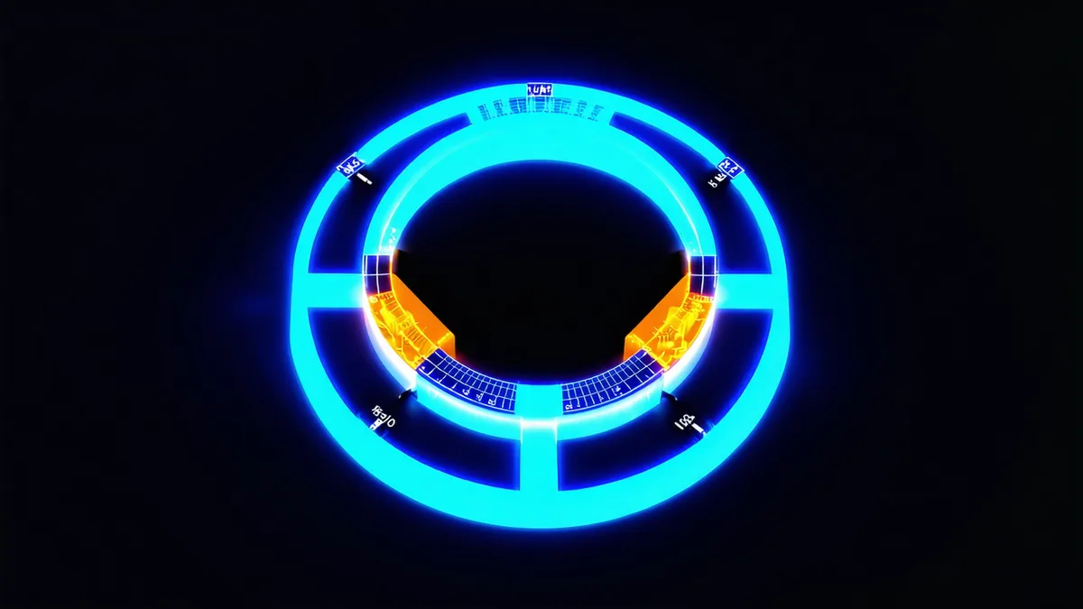
Ring Resonator Layout Verification: Radius, Coupling Gap, and Waveguide Matching

Micro-ring resonators are among the most layout-sensitive components in a PIC. Three geometric parameters determine whether a ring resonates where your simulation predicted.

ring resonatorlayout
CI/CD for PIC tape-out
Dec 5, 202511 min
CI/CD Principles Applied to PIC Tape-Out: Building a Design Review Pipeline

Software teams have automated testing. Why should photonic design teams tape out without equivalent automated review gates?

CI/CDautomation
Adiabatic taper verification
Oct 31, 20258 min
Verifying Adiabatic Taper Designs: Angle, Length, and Mode Conversion

Linear and adiabatic tapers are everywhere in PIC layouts. The geometric parameters that determine mode conversion efficiency are all checkable at the layout level.

taper designmode conversion
KLayout Python API
Sep 25, 202513 min
Automating PIC Design Checks with the KLayout Python API

KLayout's scripting interface exposes every GDS layer and cell as Python objects. Building automated design rule checks on top of this API is the foundation of modern photonic EDA workflows.

KLayoutPython
Process variation in silicon photonics
Aug 18, 202510 min
Accounting for Foundry Process Variation in PIC Verification

Silicon photonic devices are sensitive to nanometer-scale variations in etch depth and waveguide width. Verification rule decks that include fabrication corner models catch a class of failures simulation misses.

process variationfoundry
Coupling efficiency edge couplers
Jul 10, 20259 min
Coupling Efficiency Verification for Edge Couplers and Grating Couplers

The fiber-to-chip coupling point is often where loss budgets break. Automated coupling efficiency checks during layout review can flag mismatches before tape-out.

coupling efficiencyedge coupler
GDS netlist extraction PIC
May 29, 202512 min
GDS-II to Netlist Extraction in Silicon Photonics: Challenges and Gaps

Extracting a functional schematic from a GDS-II photonic layout requires recognizing optical components from geometry — a fundamentally different problem than CMOS extraction.

GDS-IInetlist extraction
PDK rule decks
Apr 29, 202510 min
What's Inside a PIC PDK Rule Deck — and Why It Matters for Verification

The PDK is the contract between designer and foundry. Understanding how layer stacks, design rules, and component models map to verification checks is the foundation of reliable tape-out.

PDKdesign rules
Optical loss budget
Mar 26, 20259 min
Building an Optical Loss Budget Before You Tape Out

Loss budget analysis is standard practice in fiber optic systems engineering. The same discipline applied to PIC design — at the layout level — prevents costly surprises at characterization.

optical lossloss budget
Mode mismatch waveguide junctions
Feb 17, 202511 min
Mode Mismatch at Waveguide Junctions: The Invisible Tape-Out Killer

A 50nm width discontinuity at a waveguide junction can scatter 15–30% of guided light. We walk through the physics and how automated verification catches it before fabrication.

mode mismatchoptical loss
LVS PIC design SPICE gap
Jan 22, 20258 min
Why SPICE-Based LVS Falls Short for Photonic Integrated Circuits

SPICE was built for electrons, not photons. Here's why the layout-versus-schematic checks that protect your CMOS designs leave critical gaps in PIC tape-out flows.

LVSSPICEverification