Built for engineers who can't afford a re-spin.
Photoniq was founded in 2021 by photonic integrated circuit engineers who had watched mode-mismatch bugs kill tape-outs at a silicon photonics research lab. Every re-spin was avoidable. The bugs were geometric — checkable from the layout, before the mask ever got made. So we built the tool we wished we had.
We're angel-backed, based in Santa Clara, CA — in the same neighborhood as the foundries and design houses we work with.
Engineers building for engineers
Four people with backgrounds in photonics physics, EDA tooling, and silicon photonics design. Everyone here has worked with or around GDS layouts and foundry tape-out flows.

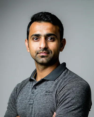
Silicon photonics researcher turned EDA tool builder. Led PIC tape-out verification work at a silicon photonics lab for 6 years before founding Photoniq in 2021.
10 years in EDA tool development. Previously built CMOS LVS engines at a major EDA vendor. Crossed over to photonics EDA when the problems got interesting.

PhD in integrated photonics from ETH Zürich. Designed eigenmode expansion algorithms for Photoniq's mode mismatch detector. Knows waveguide physics from first principles.

Former PIC design engineer at a silicon photonics foundry. Runs customer onboarding and PDK integration. If you're troubleshooting your first Photoniq job, you'll talk to David.
Every tape-out deserves a verification gate.
Software teams don't ship to production without automated testing. Photonic design teams shouldn't tape out without a verification gate either. We're building the infrastructure that makes photonic LVS as routine as CMOS DRC — because mask costs leave no room for avoidable mistakes.